
SEMICONDUCTOR REVIEW THANK YOU FOR SUBSCRIBING
× 
Semi Conductor Review Weekly Brief
Be first to read the latest tech news, Industry Leader's Insights, and CIO interviews of medium and large enterprises exclusively from Semi Conductor Review
Semiconductor Review: Specials Magazine
Goldlink
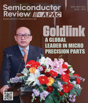
A Global Leader in Micro Precision Parts
Semiconductors power the modern world. From handheld devices to AI-driven systems, microchips form the basis for technological progress. However, before these chips can be integrated into products, they must undergo rigorous testing to ensure flawless performance. Even the smallest defect can lead to device failures, costly recalls, and reduced efficiency, making semiconductor testing an indispensable step in chip manufacturing that requires absolute precision. While chip manufacturers focus on production, companies like Goldlink play a crucial yet often overlooked role in ensuring quality. The company specializes in manufacturing ultraprecise micro parts, serving industries such as semiconductor testing, medical equipment, communications, and new energy. With advanced technology, superior quality, and shorter time to delivery, Goldlink meets the growing demand for highprecision micro parts. Goldlink is a leader in testing probe parts—the ultra-fine pins that establish reliable electrical connections between chips and testing equipment. These probes are essential for the world’s top chipmakers, ensuring that their products meet rigorous performance standards before reaching the market. By combining deep expertise in material science and precision engineering, Goldlink produces probe parts that are exceptionally durable and highly conductive, enabling accurate and efficient signal transmission during testing.
Wafer
Miraial
Advanced Wafer Handling for High-Tech Semiconductor Manufacturing
Masatoshi Hyobu, President
Miraial empowers semiconductor manufacturers with state-of-the-art wafer-handling solutions for contamination-free transport and secure storage of silicon wafers. With the industry’s rapid shift toward automation, high-quality and high-volume manufacturing, semiconductor fabs require handling solutions that align with evolving manufacturing processes. Miraial works directly with device makers to understand their requirements and develop precision-engineered wafer-handling systems. Its front-opening unified pods (FOUP), front-opening shipping boxes (FOSB) and wafer cassettes protect wafers from contamination and mechanical stress throughout their handling process. Tailoring these products to specific wafer sizes, thicknesses, and material compositions enhances production reliability and contamination control. These precisely engineered solutions integrate seamlessly into next-generation fabrication processes and enable fabs to maintain the most rigorous cleanliness and quality control standards. “As a customer-centric company, we highly value customer feedback, which is integral to our product development and quality improvement,” says Takamasa Kato, executive director. The rising demand for advanced, high-performance chips pushes semiconductor companies to refine their material handling processes, requiring more sophisticated solutions. Governments and industry leaders worldwide are strengthening domestic semiconductor capabilities. As companies restructure supply chains to meet evolving demands, Miraial’s customer base is shifting, driving demand for innovative handling solutions. To navigate this changing landscape, Miraial continuously tracks technological advancements, customer requirements and geopolitical shifts. It refines its strategy by analyzing the market, emerging manufacturing hubs and evolving material handling needs. At the heart of Miraial’s success lies an uncompromising commitment to Japanese quality, a standard that reflects meticulous engineering, stringent quality control and an obsession with purity. It partners with top global chemical firms to source high-performance plastics with ultra-low particle levels and minimal ion contamination. Setting it apart is its in-house development of molding machines, a rare capability that allows for complete control over quality and performance. “We continuously refine our strategies and set clear goals to stay competitive in this fast-evolving industry,” says Rakhmatullo Mamatov, global sales & marketing specialist..
Semiconductor AI

Ichor Systems (NASDAQ: ICHR)
Pushing The Boundaries Of Semiconductor Manufacturing
Jeff Andreson, CEO
Ichor Systems has raised the bar for custom semiconductor manufacturing with the use of exotic materials like Inconel and Hastelloy. The company provides OEMs with critical fluid delivery subsystems and components for advanced semiconductor equipment. It consistently invests in R&D to enhance its product offerings and create a level of craftsmanship that blends functionality with innovation. “Instrumental to our ability to achieve our financial performance targets are the new proprietary product introductions and customer qualifications now underway, which continue to yield positive traction and momentum,” says Jeff Andreson, CEO. Precision Ingrained in Every Offering Ichor’s portfolio includes gas and chemical delivery systems that are cost-effective and engineered to operate flawlessly in high-stakes environments, demonstrating the integrity of its production process. The gas delivery subsystems are designed to monitor and control precise quantities of specialized gases required for processes like etching and deposition. Its chemical delivery systems excel at blending and dispensing reactive liquid chemistries for applications like chemical-mechanical planarization, electroplating and cleaning. Beyond fluid delivery setups, the company offers a comprehensive range of precision-manufactured components, including precision-machined parts, electron beam and laser welded components, and precision vacuum and hydrogen brazing. The designed modules are tested in real time during the early stages of the development method, often with live process chemistries. The exceptional quality and reliability of its products have set the industry benchmark in the semiconductor space. The Talon Modular System gas delivery system is the only platform capable of supporting all popular connections like face seal, C-seal and W-seal configurations while being much smaller than conventional gas panels. The framework’s integrated heating systems offer improved operational efficiency. Its proprietary TMX C-Seal is designed to enhance productivity by improving sealing rates and reducing maintenance requirements. Ichor’s integrated manufacturing facilities and engineering hubs across the globe offer expertise in areas like orbital welding and rapid prototyping for complex projects. Its highly-trained engineers create test procedures that simulate end-user conditions to ensure reliability and production readiness. The company also offers Class 100 and Class 10,000 clean room facilities for customer-specified testing, assembly and integration of high-purity systems. It holds the exclusive international license to distribute single chamber plasma etch equipment for metal, conductor and dielectric applications.
Semiconductor Manufacturing

Driving Innovation in Automotive Systems
Fatin Farhanah Haridan, Program Development Manager, Engineering, Automotive Systems Division, Bose
Semiconductor Manufacturing

Transforming Semiconductor Manufacturing Through Expertise
Soomneck Echeng, Wafer Sort & Trim Director, Analog Devices
Wafer

Long-Standing Lean Thinking
Stewart Johnstone, Vice President Asia, Adient
Semiconductor Manufacturing

Sustainable Marketing Management and Strategic Partnership Insights
Dewi Fitriyati, Head of Business Development, PT Katolec Indonesia
Semiconductor Manufacturing

Making Things Easier in Industry 4.0 With Autonomous Mobile Robots (AMRS)
Andrew J. Wong, Head of Business Development, APAC, Continental

IN MY OPINION
Sensor
Rapidly Moving Market of Semiconductor Packaging
Cherie Sasan, Head of Design and Development, Power Module Technology, Integrated Micro- Electronics, Philippines [PSE: IMI]

LAST WORD
Sensor
Presentation Techniques for Financial Presentations
Ian Wong, Director, Financial Planning and Analysis (FP&A), Johnson Electric
IN FOCUS

Positioning APAC at the Forefront of Industry 5.0 and Quantum Semiconductor Solutions
In the rapidly evolving technology landscape, semiconductor manufacturing remains a fundamental pillar, driving global innovation.
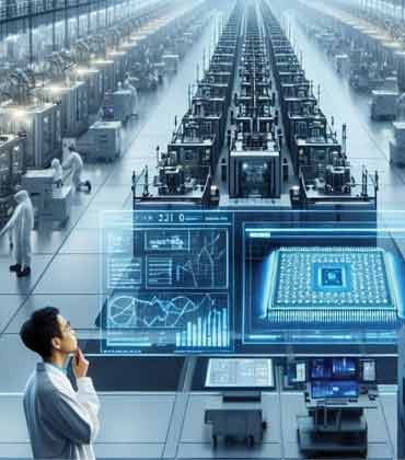
The Critical Role of Wafer Handling in the Asia-Pacific Semiconductor Industry
The Asia-Pacific (APAC) region stands as the undisputed leader of the global semiconductor industry.
EDITORIAL
Advancing Wafer and Chip Management
Wafer handling and semiconductor chip manufacturing solutions are advancing rapidly as device complexity grows and production demands intensify. Fabricators no longer see automation and precision tools as optional upgrades but as essential systems to maintain yield and reduce downtime. Shrinking nodes and growing task counts lead producers to adopt smarter systems for steady process performance.
The key technology trends driving the expansion are advanced robotics, AI-driven inspection and smart material handling systems. Advanced robotics increases precision and reduces wafer damage during transport, enabling consistent throughput in high-volume manufacturing. AI-driven inspection detects sub-micron defects in real time, improving yield and reducing manual intervention. Smart material handling systems automate wafer flow across process tools, optimizing cleanroom logistics and minimizing contamination risks through predictive coordination and environmental monitoring.
This edition of Semiconductor Review APAC explores the evolving landscape of wafer handling and semiconductor chip manufacturing solutions, highlighting key trends, innovations and strategies that help manufacturers meet rising performance demands and production complexity
It features thought leadership articles from industry experts. Andrew J. Wong, Head of Business Development, APAC at Continental, shares insights on how equipped with advanced sensors AI, and ML capabilities play a pivotal role in optimizing industrial processes. Stewart Johnstone, vice president asia at Adient, discusses how lean and reducing waste always brings the dual benefits of consuming fewer resources in operations, supporting the impact on the environment
We hope this edition, featuring Wafer Handling Solutions and Semiconductor Chip Management Solutions, helps you discover the best technologies to streamline operations and improve productivity.
This content is copyright protected
However, if you would like to share the information in this article, you may use the link below:
https://www.semiconductorreviewapac.com/edition/may-2025-12.html