

Thank you for Subscribing to Semiconductor Review Weekly Brief
× 
Semi Conductor Review Weekly Brief
Be first to read the latest tech news, Industry Leader's Insights, and CIO interviews of medium and large enterprises exclusively from Semi Conductor Review
Atotech has been recognized by Semiconductor Review Magazine as the exclusive recipient of “Advanced Semiconductor Plating Technology Company of the Year in APAC 2026,” based on our proprietary methodology, reflecting its position in the industry, and is also named among “,” reflecting its broader leadership. This profile has been developed by the Semiconductor Review research and editorial team based on insights from an interview with John T.C. Lee, MKS President and CEO.

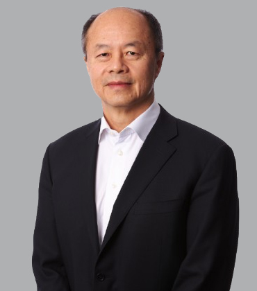 John T.C. Lee, MKS President and CEO
To sustain performance growth, the industry is embracing heterogeneous integration and advanced packaging. Rather than relying on a single monolithic chip, advanced packages integrate multiple specialized dies into a unified system. This approach is becoming essential for AI, HPC, mobile, automotive and next-generation communications applications. Increasingly, future performance gains will depend as much on packaging innovation as on silicon innovation.
From Transistor Scaling to System Integration
The AI era is defined not only by more powerful algorithms, but by the infrastructure required to support them. System performance increasingly depends on how efficiently devices are integrated, interconnected, powered, cooled and manufactured at scale.
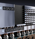 As Moore's Law slows, innovation is shifting toward advanced packaging and precision interconnect engineering.
Packaging is no longer a final assembly step. Packaging is performance
At the center of this transition is the interconnect stack, spanning multilayer PCBs, high-density interconnect (HDI) boards, package substrates, silicon interposers, GPUs and high-bandwidth memory (HBM). Signal integrity, thermal management, contamination control, dimensional accuracy and yield must all be optimized simultaneously to enable AI systems to scale.
Manufacturing Challenges in the AI Era
The increasing complexity of AI and HPC architectures introduces several key challenges:
• Growing package sizes and I/O density driven by larger HBM configurations and heterogeneous integration.
• Smaller interconnect geometries requiring ever-greater precision in routing, plating and bonding.
• More stringent requirements for reliability and contamination control.
• Rising thermal loads and power densities.
• Material compatibility and substrate warpage challenges.
• Increasing pressure to improve energy efficiency and sustainability.
• Greater design complexity spanning chip, package and system levels.
• The need to increase manufacturing yield while controlling costs.
As these factors become increasingly interdependent, optimizing individual process steps in isolation is no longer sufficient.
From Device Scaling to Interconnect Optimization
Future semiconductor performance gains will increasingly be driven by advances in interconnect technology.
Modern AI architectures rely on a hierarchy of interconnected structures spanning PCBs, package substrates, silicon interposers, memory stacks and advanced packaging. Success depends on simultaneously optimizing bandwidth, power delivery, thermal performance, contamination control, reliability and yield.
As AI architecture becomes more sophisticated, yield and performance increasingly depend on the seamless coordination of multiple technologies.
This reality is driving closer collaboration across the entire ecosystem, including materials suppliers, equipment manufacturers and semiconductor technology providers. Success increasingly depends on integrating expertise in materials science, laser processing, plating chemistry, plasma technologies, vacuum engineering, metrology, analytics and process control.
MKS refers to this system-level philosophy as Optimize the Interconnect℠.
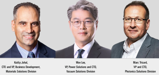 Building on the company's Surround the Wafer® and Surround the Workpiece® strategies, Optimize the Interconnect℠ aligns materials, manufacturing equipment, photonics, laser technologies, vacuum solutions and process control into integrated manufacturing solutions. The goal is not to optimize individual steps, but to maximize the performance, reliability, scalability and yield of the complete interconnect architecture.
Building the AI Stack
At the system level, AI infrastructure relies on high-layer-count PCBs to distribute power and high-speed data through increasingly dense copper networks. As current densities and signal speeds rise, precision laser drilling, uniform copper plating and advanced process control become critical.
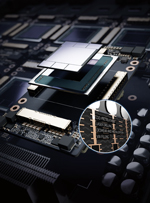 Within these board architectures, HDI technology enables increasingly dense routing and interconnection. Consistent surface treatment, metallization, laser processing and plating are essential to maintain reliability.
Package substrates provide the bridge between board-level routing and silicon-level precision. As I/O counts and HBM stack heights increase, overlay accuracy, warpage control and contamination-free processing become increasingly important.
At the heart of AI bandwidth scaling is the silicon interposer, connecting GPUs and stacked memory through ultra-fine interconnects including through-silicon vias (TSVs). As leading-edge architectures increasingly adopt copper-to-copper hybrid bonding, manufacturing demands increase further, requiring ultra-flat surfaces, atomically clean interfaces and highly controlled deposition environments.
At the top of the stack, GPUs and HBM towers operate under extreme power densities. Here, thermal management, thin-film precision and contamination-free processing directly influence performance, efficiency and long-term reliability.
Integration as Strategic Differentiation
Many companies contribute individual technologies to AI infrastructure, including production equipment, chemistries, laser systems, vacuum solutions, metrology and process control tools.
MKS differentiates itself through its ability to integrate and optimize across these domains.
-
The next decade of AI growth will be driven by higher data-center density, larger HBM stacks, more advanced packaging architectures and increasing demands for energy efficiency.
Its advanced materials portfolio enables ultra-fine copper interconnect formation, diffusion barrier control and surface preparation for high-density routing and hybrid bonding. Its photonics technologies support precision via formation, material structuring and scalable manufacturing. Its vacuum solutions provide the pressure control, gas-flow management, plasma activation and contamination mitigation required for advanced packaging and thin-film processes.
 By combining these capabilities, manufacturers can address complexity holistically rather than as a series of disconnected manufacturing steps.
As AI architecture becomes more sophisticated, yield and performance increasingly depend on the seamless coordination of multiple technologies. MKS's Optimize the Interconnect℠ approach provides a framework for aligning materials, equipment and process expertise into integrated manufacturing solutions.
Enabling the Future of AI Infrastructure
The next decade of AI growth will be driven by higher datacenter density, larger HBM stacks, more advanced packaging architectures and increasing demands for energy efficiency.
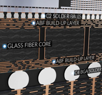 Glass substrates, panel-level packaging, photonics integration, thermal management and power delivery are all emerging as critical technology frontiers. Across each of these areas, precision at scale will be a key competitive differentiator.
MKS's role is to enable that precision across every layer of the AI hardware stack. By combining materials science, photonics innovation, laser processing, advanced manufacturing equipment and precision vacuum technologies, MKS helps manufacturers overcome growing challenges in density, thermal management, contamination control, reliability and yield.
AI does not scale on algorithms alone. It scales on infrastructure.
It scales on the invisible layers of copper, silicon, surface chemistry, laser processing, advanced packaging and vacuum-controlled environments that connect, power and cool the system.
As AI continues to transform industries and societies, MKS stands at the foundation of that transformation, enabling the interconnect technologies that power the infrastructure of intelligence.
Advanced Semiconductor Plating Technology Companies in APAC Info
Q1
What Does Advanced Semiconductor Plating Technology Contribute to Modern Chip Manufacturing?
Advanced Semiconductor Plating Technology deposits conductive and functional metal layers onto semiconductor structures, helping manufacturers build increasingly complex devices. These processes form electrical connections and interconnects used in advanced packaging, where metal purity, even deposition and reliable filling affect performance. More compact chip designs call for plating that can handle finer structures and tighter tolerances. Common methods include electroless and electrolytic deposition, copper pillar formation, redistribution layer (RDL) plating and through-silicon via (TSV) metallization.
Q2
How Does Atotech Apply Advanced Semiconductor Plating Technology Across Different Applications?
Atotech brings together wet chemical processes, production equipment and technical services for semiconductor manufacturing. Its work in Advanced Semiconductor Plating Technology spans several packaging and interconnect applications. Its portfolio covers pad metallization, copper pillar plating, redistribution layers, vias and dual damascene applications. The company supports power semiconductor manufacturing and advanced packaging, including fan-out wafer-level packaging (FOWLP) and flip-chip chip-scale packaging (FC-CSP). Its Spherolyte® Cu UF3 process supports high-purity copper deposition for fine-line redistribution layers and micro-via filling. These processes address the interconnection demands of advanced semiconductor packages.
Q3
Which Plating Processes Matter in Advanced Semiconductor Packaging?
Different package designs call for different deposition methods. Copper pillar plating forms conductive structures between chips and packages, while RDL plating extends electrical connections across a package surface. Micro-via and TSV plating connect layers, including in structures used for three-dimensional integration. Advanced Semiconductor Plating Technology must also support adhesion, solderability and controlled metal deposition. The right process depends on package architecture, feature dimensions, electrical requirements and compatibility with later manufacturing steps.
Q4
How Does Material Purity Affect Semiconductor Plating Performance?
Impurities and uneven deposits can weaken conductivity, adhesion and long-term package performance. Material purity therefore matters alongside the consistency of the metal layer. Advanced Semiconductor Plating Technology relies on controlled chemical formulations and stable process conditions, particularly in fine-line copper applications. Deposition uniformity and reliable feature filling help protect interlayer connections, where small variations can affect the finished structure. High-purity chemistry, controlled bath conditions and suitable equipment configurations all contribute to repeatable production.
Q5
How Does Atotech Support More Complex Semiconductor Manufacturing Requirements?
Atotech pairs chemical processes with specialized equipment, software and technical support. Its electroless deposition processes cover pad metallization and RDL housing, while electrochemical deposition is used for pillars and vias. The company also works with dual damascene solutions for advanced interconnect structures. Its research and development work and global technical center network support material science investigations and process development. In Advanced Semiconductor Plating Technology, this work focuses on deposition characteristics, production efficiency and manufacturing reliability.
Q6
What Should Manufacturers Evaluate When Selecting Semiconductor Plating Solutions?
A suitable process must fit the device architecture and the requirements of the package being produced. Manufacturers can compare deposition uniformity, chemical purity, feature-filling performance, process compatibility and production consistency. Advanced Semiconductor Plating Technology may serve power chips, memory, logic devices or advanced packaging, so the intended application should guide the assessment. Equipment integration and access to technical assistance also matter, particularly when specifications change. Evaluating chemistry and equipment together helps manufacturers weigh process control, production costs and reliability.
| Share this Article:Tweet
|
Company
Atotech
Management
John T.C. Lee, MKS President and CEO
Description
MKS provides advanced manufacturing equipment, components, subsystems and process solutions that enable innovation across semiconductor, electronics and industrial markets. Combining expertise in materials science, photonics, laser technologies, vacuum systems and process control, MKS supports precision manufacturing and next-generation technology development.
This content is copyright protected
However, if you would like to share the information in this article, you may use the link below: