
SEMICONDUCTOR REVIEW THANK YOU FOR SUBSCRIBING
× 
Semi Conductor Review Weekly Brief
Be first to read the latest tech news, Industry Leader's Insights, and CIO interviews of medium and large enterprises exclusively from Semi Conductor Review
Semiconductor Review: Specials Magazine
Semiconductor devices form the bedrock of our increasingly connected world, powering the technologies that are reshaping our lives – from the sophisticated algorithms of artificial intelligence to the immense processing power of high-performance computing servers and the seamless connectivity of autonomous vehicles. For decades, the relentless march of Moore's Law, with its promise of doubling transistor density roughly every two years, fueled unprecedented progress in cost per function. This historical advancement, driven by Dennard scaling and multi-core architectures, now faces headwinds as traditional transistor scaling slows, creating a critical crossroads for the industry to maintain the economic viability of future innovations. To counter this slowdown, the semiconductor industry is strategically pivoting towards heterogeneous integration and advanced packaging. This paradigm shift moves beyond encapsulating a single chip to integrating multiple specialized dies into a unified package that operates as a cohesive system. It offers a modular approach to increasing input/output density and sustaining performance gains in electronic devices, effectively extending the trajectory of progress beyond the limitations of traditional scaling – a concept often dubbed "More than Moore's Law." This technology is no longer niche; it is becoming indispensable across a vast spectrum of microelectronics applications, from the power-hungry AI and HPC servers demanding colossal processing power and high-bandwidth memory to the size, weight, and power-conscious requirements of mobile devices. The diverse and evolving demands of these applications are continuously propelling the innovation and refinement of advanced packaging architectures and process technologies. This transition is not without its challenges. The increasing complexity of advanced packages, driven by the demands of AI, renewable energy systems, autonomous vehicles, and other high-performance applications, presents significant hurdles in manufacturing spanning several critical areas. Current challenges in semiconductor manufacturing: • Larger package sizes and increased I/O density: The insatiable appetite of AI and HPC for computational power and memory bandwidth necessitates larger package sizes to accommodate a greater number of HBM stacks. This trend, coupled with the move towards 3D heterogeneous integration on interposer combined with a package substrate, demands innovative materials and processes capable of handling increased complexity and stringent performance requirements. • Shrinking feature sizes and interconnect pitch: Next-generation chip designs rely on increasingly higher I/O densities, pushing the boundaries of interconnect technology and requiring significantly smaller pitches. Micro bumps are reaching their limitations, necessitating the exploration and adoption of advanced interconnect solutions like Cu-Cu hybrid bonding. • Reliability and contamination control: As packages become more complex with finer features and multiple integrated dies, ensuring long-term reliability and stringent contamination control throughout manufacturing becomes paramount. This is particularly critical for demanding applications like automotive and aerospace. • Thermal management: The increasing power density within advanced packages, driven by the integration of more dies and passive components, poses a significant thermal management challenge. Efficiently dissipating the generated heat is crucial for maintaining performance and reliability. • Material compatibility and warpage: Integrating diverse materials with varying thermal and mechanical properties in advanced packages can lead to issues like warpage, especially with larger substrate sizes. This necessitates the exploration of new substrate materials such as glass, which offer superior thermal stability but require novel processing techniques. • Energy efficiency and sustainability: The exponential growth of AI and data centers is driving tremendous energy demands. Enhancing energy efficiency at every level – from the chip design to the manufacturing process – and adopting sustainable manufacturing practices are becoming increasingly critical. • Design complexity and tooling: Designing and optimizing complex 3D heterogeneous packages requires sophisticated tools and methodologies that can handle multi-physics domains. The current disconnect between chip-level and package-level design kits adds to this complexity. • Manufacturing cost and yield: Achieving cost-effective manufacturing with high yields for these complex advanced packages remains a significant challenge. This requires continuous innovation in materials, equipment, and processes.
Top Silicon Wafers Solution in APAC 2025
As semiconductor technologies advance and R&D cycles accelerate, there’s a growing need for high-quality, small-volume test wafers that support rapid process development and materials validation. For semiconductor equipment manufacturers and materials suppliers offering high-purity gases and specialty chemicals, these wafers provide a cost-effective way to simulate real manufacturing conditions without committing to large-scale fabrication runs. However, sourcing these test wafers for early-stage research is a persistent challenge. Traditional wafer suppliers are built for high-volume production, not the flexibility and responsiveness that early-stage research demands. Micro Semiconductor Research (MSR) was founded to close that gap. Specializing in low-volume, high-complexity wafer solutions, MSR plays a vital role for R&D teams in semiconductor equipment and materials companies. These innovators rely on high-quality wafers to simulate real production environments, whether calibrating etch and deposition tools or testing the purity of specialty gases and chemicals. Offering customized wafer processing, including refurbished prime silicon and advanced bonding capabilities, MSR enables rapid iteration, precise validation, and true development freedom. Where others require high minimums and rigid specs, MSR delivers flexibility, speed, and deep technical insight.

CXO INSIGHTS

Accelerate the Semiconductor Workflow with a Standardized Measurement Framework
Mike Watts, Head of Industry Marketing, Semiconductor and Electronics, NI (National Instruments)

Recruitment Challenges in the HighTech Packaging World
August Miller, Director, R&D Design Center and Daniella Olson, Staff Engineer, Amkor Technology, Inc

Connecting Dots
Kevin Anderson, Director Integration Technology Research, Qorvo, Inc

Unlocking the true value of Data - Lessons from the journey
Adarsha Marpalli, Sr Director- Global Head Data and Insights, Nexperia

Industry 4.0: Navigating Disruptive Technologies in Manufacturing
Peter Chambers, Senior Director, OEM Sales APJ & Country Manager, Australia, AMD [NASDAQ: AMD]


IN FOCUS

The Critical Role of Wafer Handling in the Asia-Pacific Semiconductor Industry
The Asia-Pacific (APAC) region stands as the undisputed leader of the global semiconductor industry.
EDITORIAL
The Next Era of Semiconductor Innovation
Semiconductor manufacturing is advancing rapidly to power the next generation of technologies, from AI-driven devices to electric vehicles, driving unprecedented global demand. As production volumes surge and chip complexity grows, fabs must adopt solutions that optimize operations and provide the agility to navigate shifting market pressures. Backed by precision control and real-time data insights, these solutions empower fabs to make faster, smarter decisions, ensuring consistent delivery of highperformance chips.
Reports highlight that the APAC semiconductor device market, valued at $504.99 billion in 2025, is projected to reach $753.76 billion by 2030 at a CAGR of 8.34 percent.
Fueling this growth are some advanced technologies. IoT enables continuous process monitoring and predictive maintenance, boosting efficiency and reducing downtime. AI accelerates chip design and production workflows, facilitating the creation of high-performance processors tailored for complex applications. Advances in materials technology allow for smaller, more durable and energy-efficient chips that perform reliably under demanding conditions.
This edition of Semiconductor Review APAC presents expert perspectives on how innovation is shaping the semiconductor sector’s future. It features insights from Matthew Yap, sr. manager of design engineering at Microchip Technology Inc., who highlights how AI or machine learning offers powerful opportunities to boost engineering productivity and scalability in IC design while maintaining the essential role of human engineers. Adarsha Marpalli, Sr. directorglobal head data and insights at Nexperia, emphasizes that to unlock true value from AI, machine learning and data, companies must prioritize data literacy and modern tools. He also underscores the need for a cultural shift that treats data as a core asset across the organization.
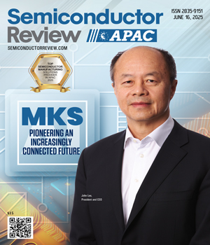
The magazine also features MKS, a leading provider of integrated technologies for advanced semiconductor and electronics packaging, specializing in plating, laser processing and surface modification.
We hope this edition sparks new ideas and offers practical perspectives as you navigate the industry’s challenges and opportunities.
This content is copyright protected
However, if you would like to share the information in this article, you may use the link below:
https://www.semiconductorreviewapac.com/edition/16-june-2025-15.html