
SEMICONDUCTOR REVIEW THANK YOU FOR SUBSCRIBING
× 
Semi Conductor Review Weekly Brief
Be first to read the latest tech news, Industry Leader's Insights, and CIO interviews of medium and large enterprises exclusively from Semi Conductor Review
Semiconductor Review: Specials Magazine

Radio frequency (RF) and microwave systems are the backbone of modern communications, bridging the digital and physical worlds. Their performance hinges on materials like silicon, gallium nitride (GaN), and indium phosphide (InP)—each offering distinct advantages: silicon for cost-effectiveness, GaN for high power and efficiency, and InP for ultra-high-speed communication. However, integrating these materials into a single system poses significant challenges due to differences in lattice structures, thermal properties, fabrication processes, and costs. PseudolithIC, a pioneer in heterogeneous integration, addresses this challenge with true chiplet-level integration on a common silicon CMOS wafer. By uniting diverse semiconductor materials and functionalities into a single platform, the company enables seamless and scalable transitions from monolithic architectures to modular, high-performance RF systems on a chip (RF SoC). PseudolithIC is on a mission to commercialize cutting-edge compound semiconductor technologies, serving a wide range of markets—from wireless infrastructure and SATCOM to quantum computing and defense applications. “Specializing in heterogeneous technology, we go beyond just combining different materials,” says Florian Herrault, CEO and co-founder. “Our IP revolves around both design and fabrication, leveraging the highest-performance transistors from leading-edge compound semiconductor foundries while developing intelligent circuits on a cost-effective silicon CMOS platform that can scale efficiently.” The Perfect Blend of GaN and Silicon Since cost is a major concern for businesses adopting heterogeneous integration, PseudolithIC offers a ready-made solution that doesn’t compromise on performance. The company has developed a digital and physical library of standardized chiplets made from compound semiconductor materials, significantly reducing prototyping expenses. Using these chiplets, it can design and test RF circuits in silicon in as little as three months—enabling faster iteration than traditional monolithic circuit technologies. Building on this foundation, PseudolithIC’s next-generation RF and millimeter-wave chipsets incorporate silicon to further improve cost-efficiency. The precision of silicon transistor and passive element modeling ensures higher first-pass success rates in prototyping, enhancing overall productivity.

Specialty Ffkm Materials Manufacturing Company of The Year 2025
Are perfluoroelastomer (FFKM) seals the ideal solution for harsh semiconductor manufacturing environments? FFKM seals are widely adopted for their exceptional resistance to gases like nitrogen trifluoride and tetrafluoromethane, commonly used in plasma etching, ashing and deposition processes in semiconductor manufacturing. Despite their chemical durability, they remain susceptible to mechanical damage. In environments where even the slightest leak can compromise yield, effective sealing demands more than just chemical resistance. Applied Seals N.A., Inc (ASNA) takes a fundamentally different approach to FFKM sealing. Rather than simply providing general-purpose FFKM parts, ASNA equips toolmakers and process engineers with deep engineering insights. It identifies what’s truly needed, not just what’s requested, and educates customers on how FFKMs behave under real-world thermal, chemical and mechanical stress. “We don’t just sell seals, we teach the science behind them. That’s how we change the outcome,” says Dalia Vernikovsky, CEO. Engineering the Right Seal for Every Fab ASNA Calculated Engineering (ACE®), its proprietary engineering platform, is designed to optimize the key conditions for reliable sealing performance. With ACE®, engineers can validate groove dimensions, environmental variables and hardware configurations to ensure proper fit and function. Building on this foundation, ASNA employs realistic data-based on finite element analysis (FEA) to optimize seal performance by minimizing physical stresses, as well as surface exposure to heat and chemicals. Its world-class engineering team analyzes stress and strain across specific applications to recommend the most suitable compounds and custom geometries. This integrated, data-driven approach enhances sealing integrity, extends component lifespan and enables predictability of reliable performance under real fabrication facility (fab) conditions. A cornerstone of ASNA’s strategy is its proprietary PERFREZ® line of FFKM compounds, engineered specifically for the harshest semiconductor processes. PERFREZ® materials are optimized for high-energy plasma, thermal cycling and aggressive wet chemicals such as HF, SC1 and sulfuric acid. Their formulation offers exceptional erosion resistance and low particle shedding—key for protecting wafer integrity in ultra-clean environments. Combined with ASNA’s precision molding capabilities, PERFREZ® seals retain their shape, resist compression set and maintain mechanical strength under the high-vacuum, high-temperature conditions, typically seen in most advanced semiconductor tools..

Top PCB Assembly Service 2025

Tech e-Services is a one-stop shop for high-quality electronics manufacturing. Specializing in high-mix, low-to-mid volume production, it offers seamless solutions across PCB assembly, precision cable and wire harnesses, prototyping, testing, fulfillment and product repair. All services are delivered under a white-label model that safeguards and reinforces clients’ brand identity. A family-owned business, iTech e-Services started as a 1,500-squarefoot repair shop and has grown into a 45,000-square-foot ESD-certified facility offering full-spectrum electronics manufacturing services. From its early focus on electronics repair, it has evolved into a trusted partner to industries including aerospace, medical, industrial and technology, delivering complete solutions while staying true to the values that shaped its foundation. Whether clients provide a BOM, gerber files or technical drawings, the team handles sourcing, production, logistics and RMA management to ensure smooth execution from concept to delivery. Built on integrity, hands-on problem-solving and faith-driven values, the company blends personal commitment with process discipline to deliver quality clients can trust at every stage. Backed by AS9100D certification for aerospace and ISO 13485 for medical device manufacturing, iTech ensures traceability and repeatable performance at every stage. From the first unit off the line to the millionth, the same rigorous standards apply. “Every investment we make, in people, process and equipment, is to ensure repeatable quality our customers can trust,” says Racheal Ho-Tran, owner. The focus on purposeful investment comes to life on the production floor, where advanced manufacturing technology drives precision at every step. iTech runs three fully integrated SMT lines with a combined placement capacity of 75,000 components per hour. Each line supports a fully automated workflow, from solder paste inspection to X-ray, automated optical inspection and in-circuit testing. A flying probe tester adds high-precision inspection for complex or low-volume builds. Every machine is carefully selected for accuracy and maintained through annual calibration, ensuring a tightly controlled environment for reliable, error-free builds that deliver on iTech’s promise of precision and peace of mind.
Top Semiconductor Equipment Refurbishment Service 2025
The semiconductor industry is booming, driven by surging demand for advanced chips in AI, electric vehicles, consumer devices, and renewable energy. Fabs often find their growth stalled by the capacity constraints for systems meant to propel them. New OEM equipment requires hefty capital outlays and often results in long lead times as suppliers prioritize their largest customers. Once installed, generic support and one size fits all servicing slows production qualification and fail to meet customer requirements. These obstacles demand solutions as cutting edge as the chips themselves, tailored to each fab’s needs. One company meeting that need is Semicat, a provider of high performance PVD systems with more than 20 years of industry experience. Semicat refurbishes and manufactures tools to OEM standards, leading in EnduraTM and CenturaTM platform refurbishment. It adheres to rigorous testing protocols and Best Known Method (BKM) practices across both 200mm and 300mm PVD systems. These stringent quality controls ensure each refurbished or newly built tool performs reliably, meeting or exceeding original OEM standards before delivery. Each tool delivered by Semicat, whether refurbished or newly built, is engineered to match OEM performance specifications in hardware and process capability. This focus on quality, combined with faster lead times and personalized customer support, allows fabs to scale operations without sacrificing reliability. “Our commitment is simple: we deliver the same performance as a brand new system. Customers should not have to choose between speed, cost, or quality. They can have all three,” says Mike Nam, CEO. Semicat delivers real world results by cutting lead times by up to 50 percent, enabling fabs to respond swiftly to demand surges and gain a competitive edge. For example, when a 300mm Singapore fab faced capacity constraints and a delayed OEM system orders, Semicat configured and delivered the required systems to meet customer’s schedule. The fab met its production timeline, and the customer praised Semicat for performance, cost savings, responsiveness, and reliability throughout the process.

CXO INSIGHTS

Recruitment Challenges in the HighTech Packaging World
August Miller, Director, R&D Design Center and Daniella Olson, Staff Engineer, Amkor Technology, Inc

Rapidly Moving Market of Semiconductor Packaging
Cherie Sasan, Head of Design and Development, Power Module Technology, Integrated Micro- Electronics, Philippines [PSE: IMI]

Harnessing the Power of Additive Manufacturing to Advance Semiconductor Capital Equipment Performance
Scott Green, Director Advanced Software R&D, 3D Systems Corporation

Crafting the Future with AI, Cloud and Operational Excellence
Damian Ng, SVP of Technology, Head of Enterprise Architecture, Software Engineering, Reliability and Operations, Anywhere Real Estate Inc

Acceleratethe Semiconductor Workflow with a Standardized Measurement Framework
Mike Watts, Senior Solutions Marketer for Semiconductor Validation, NI

IN FOCUS

Heterogeneous Integration: The Key to Future-Ready Semiconductors
Heterogeneous Integration (HI) is quickly becoming a cornerstone of innovation in the semiconductor industry.
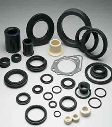
Specialty FFKM Materials: Enhancing Reliability in High-Tech Industries
The specialty FFKM materials manufacturing market is poised for continued growth, underpinned by its critical role in high-purity and high-performance environments.
EDITORIAL
The Connected Value Chain of Semiconductors
The semiconductor industry is entering an era where progress is no longer measured solely by node shrink or transistor density. Today, innovation lies in the seamless orchestration of multiple disciplines, where advanced materials, precision manufacturing, and intelligent system integration converge to redefine performance, reliability, and scalability.
At the core of this transformation is heterogeneous integration technology, combining diverse components, from logic and memory chips to sensors and photonics, into unified systems. This approach moves beyond traditional scaling, enabling engineers to achieve higher functionality and efficiency without sacrificing form factor. Yet, to make such intricate architectures possible, the supporting materials and processes must be equally advanced.
This is where specialty FFKM (perfluoroelastomer) materials manufacturing plays a pivotal role. Known for exceptional chemical and thermal resistance, these materials are critical in semiconductor fabrication environments, where equipment operates under extreme conditions. FFKM seals and components safeguard process integrity, ensuring that the delicate layers in integrated devices are produced without contamination or compromise.
As these chips transition from wafer to fully functional systems, the expertise of PCB assembly services becomes critical. Highprecision assembly is not just about soldering components onto a board; it’s about aligning electrical, thermal, and mechanical requirements so that advanced semiconductor devices can function flawlessly in real-world applications. Every interconnect, trace, and joint must uphold the performance embedded in the chip design.
Completing the chain are semiconductor equipment solutions, the tools and systems that enable consistent, repeatable, and scalable manufacturing. From wafer processing to final testing, these solutions embody the fusion of engineering disciplines, ensuring that cutting-edge designs can be produced reliably and in volume.
When viewed collectively, these four domains form a tightly linked value chain that is shaping the semiconductor industry’s future. Heterogeneous integration sets the vision. Specialty FFKM materials make extreme manufacturing environments viable. PCB assembly turns micro-scale innovation into functional products. Semiconductor equipment solutions power the journey from concept to reality.
This content is copyright protected
However, if you would like to share the information in this article, you may use the link below:
https://www.semiconductorreviewapac.com/edition/august-2025-21.html