
SEMICONDUCTOR REVIEW THANK YOU FOR SUBSCRIBING
× 
Semi Conductor Review Weekly Brief
Be first to read the latest tech news, Industry Leader's Insights, and CIO interviews of medium and large enterprises exclusively from Semi Conductor Review
Semiconductor Review: Specials Magazine
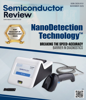
Diagnostics has always been about tradeoffs. Central laboratories deliver the highest sensitivity, but they come with delays and high infrastructure costs. NanoDetection Technology ™ (NDT) eliminates the trade-off through its next-generation diagnostic solutions for human and veterinary medicine. The innovations of NDT center on its biochip; a technology originally developed at Oak Ridge National Laboratory in Tennessee. The biochip uses chemiluminescence-based sensing that captures light signals released during chemical reactions to deliver laboratory-grade precision in a compact, point-of-care system. Unlike traditional lateral flow tests, which rely on the human eye to read faint lines, the NDT biochip detects light many times below visual thresholds—many orders of magnitude fainter than the eye can register. “Our sensitivity is such that from Earth we could catch signals as faint as the glow of a candle burning on the moon,” says Douglas Durand, CEO. The NDT biochip isn’t limited to one target at a time. Each unit contains 25 discrete light detectors, which means a single run can resolve up to 24 analytes along with a background channel. With multiplexing, entire biomarker panels can be scanned in a single run—streamlining workflows and replacing the inefficiency of test-by-test analysis. That difference matters. For a clinician in an urgent care setting, infections that would otherwise slip past a rapid test can now be detected early. For veterinarians, it means detecting disease promptly to prevent herd disease, animal mortality or a virus outbreak. Field based diagnostics can use this to bring accuracy to settings far removed from centralized labs. Capable of running approximately 25 tests per hour NDT has made advanced diagnostics not only faster, but scalable and practical across diverse environments. The design of the NDT diagnostic platform reflects an understanding of how testing is conducted in real-world conditions. Disposable test cassettes minimize the risk of contamination, streamline workflow and reduce costs. And results are produced in only minutes. “The system is optimized for chemiluminescence today, but its architecture is also compatible with fluorescence and phosphorescence,” states James Marous, Head of Engineering at NDT. “So, if a lab is buying the instrument today, they are already covered for the assay formats of tomorrow.”
Advanced Optoelectronics Company of the Year 2025
The promise of optoelectronics has always been bright. For decades, the field has promised smarter imaging, faster data transfer, and health monitoring tools that could change lives. Yet in practice, many of those promises stalled: Smartphones still struggle with under-screen facial recognition and autofocus on invasive continuous glucose monitors remain buggy and inaccurate prototypes; and traditional copper interconnects are struggling to meet exponentially increasing energy demands from the AI revolution, with data center fires and performance shortfalls becoming regular risks. For Jacob Tarn, Ph.D., CEO of InPHRED, this slowdown has been long coming—current optoelectronics are already at the limits of conventional semiconductor materials. With nearly forty years in the compound semiconductor industry, he had seen the potential of indium phosphide and gallium nitride technology, but also their shortcomings. The devices built on these material platforms could only stretch so far. That moment of recognition set InPHRED on its current path.“When I first engaged with Professor Han at Yale University on InPHRED’s nanoporous technology, I knew immediately that we had found a breakthrough that could take us beyond what conventional semiconductors had been able to achieve,” he says. InPHRED was founded on the belief that the right material innovation could unlock stalled applications across industries. By engineering nanoporous structures into semiconductors, InPHRED has managed to bend the rules of how light can be emitted and controlled. So far InPHRED has developed two families of flagship products—shortwave infrared (SWIR) vertical-cavity surface-emitting lasers (VCSELs) and resonant cavity LEDs (RC-LEDs)—but the company’s broader nanotechnology platform can transform the next generation of optoelectronics solutions. Rethinking Old Limits To understand the significance of InPHRED’s work, it helps to look back at what came before. Indium phosphide has been a workhorse in high-tech industries for more than thirty years. Its edge-emitting lasers powered telecom infrastructure and other demanding applications, but the nature of edge-emitting geometry meant that devices were expensive and complicated to manufacture, and difficult to scale. In contrast, vertical cavity surface-emitting lasers (VCSELs) have better yield, better optical properties, and can be much more manufacturable at scale. The key ingredient for VCSELs is a highly reflective mirror. For thirty years, the semiconductor industry hoped that it would be possible to build a surface-emitting indium phosphide laser—as had been achieved in gallium arsenide, a different material system. Gallium arsenide VCSELs are currently ubiquitous in consumer electronics products, but fundamental material limitations of the periodic table meant that there are no good mirrors for the indium phosphide system.

Top High Speed CMOS Image Sensors Solution 2025

Traditional image sensors flood systems with vast streams of raw data, leaving the heavy lifting to costly field programmable gate arrays (FPGAs). But Luxima Technology flips that model by embedding intelligence directly into its high speed sensors, streamlining data pipelines before they ever reach the backend. This modern approach reduces FPGA requirements, simplifies integration, and lowers system cost. More than just sensors, Luxima delivers fully integrated imaging solutions for high performance applications. By combining sensor innovation, companion components, and application-specific optimization, the company presents world-class performance in compact, power-efficient packages that surpass traditional methods. “We study each application in depth, viewing the entire system to refine elements into an image sensor, delivering more optimized solutions than traditional approaches,” says Lin Ping Ang, cofounder and CEO. Luxima’s portfolio centers on three business models: standard products, semi-custom designs, and fully custom solutions, each serving different customer needs. The standard model offers off-the-shelf high-speed CMOS image sensors for broad applications like machine vision, broadcast cameras, motion analysis, and biomedical imaging. For greater optimization, the semi-custom model involves close collaboration with customers to enhance imaging performance, cut costs, and simplify integration. These sensors may also be sold to other markets under time-limited or region-specific exclusivity, which helps reduce non-recurring engineering (NRE) fees. Lastly, the company’s fully custom solutions are designed exclusively for a single customer, fine-tuning specific parameters such as sensitivity, noise, pixel size, power, and interfaces to achieve superior, application-specific performance. Since every level of customization demands efficiency, Luxima’s design cuts out the clutter of multiple parallel channels, making sensor-to-FPGA links faster and cleaner than traditional setups. Beyond speed, the sensors also unlock advanced 3D imaging, giving developers the flexibility to create high- performance, data-rich applications. All of this comes in compact packages that keep power use low and costs under control.
Top Microdisplay Technology 2025
The display industry has progressed through LCD, DLP, OLED, LCOS, and MicroLED, powering everything from automotive dashboards and AR/VR headsets to medical and industrial devices. While these technologies have proven reliable, growing demand for smaller, more durable, and energy-efficient displays is exposing their limits. This opportunity is driving the rise of microdisplays across AR/VR, automotive, medical, and industrial applications. Many existing solutions still struggle with resolution, compactness, power efficiency, and reliability under heat and vibration, limited by legacy analog architectures that can’t keep up with modern digital demands. Syndiant, a pioneer in Liquid Crystal on Silicon (LCoS) microdisplays, and its subsidiary XDMicro form a full-stack semiconductor provider of high-resolution, low-power, compact display solutions. Building on nearly two decades of innovation, Syndiant’s LCoS microdisplays leverage precise digital control, high resolution, and low power in a compact reflective chip, delivering performance where traditional technologies fall short. Syndiant leads design and application development from its US headquarters, while XDMicro in China provides vertically integrated manufacturing, from liquid crystal to module and optical engine assembly, enabling high-volume automotive and consumer-grade products. “Unlike legacy solutions like DLP or analog LC, our focus is on delivering microdisplays that perform consistently in the real world, from next-generation AR glasses, projectors, to automotive system applications. Reliability and precision aren’t just specs—they’re essential to the experiences our customers are creating,” says Daniel Wong, President and CEO. From Design to Integration Syndiant’s LCoS microdisplays are reflective chips that modulate light to create projected images. Paired with ASIC controllers and integrated with optical engines, they form high-performance solutions for compact form factors. Syndiant’s architecture facilitates programmability, enabling manufacturers to fine-tune color and imaging performance. It also supports future advances like phase modulation for holographic displays and MicroLED development.
Top Supplier of High-Purity Metals & Compounds 2025

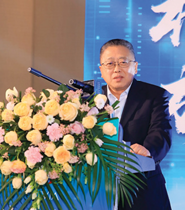
American GMG Inc. (AGMG) is a trusted global supplier of ultra-high-purity metals, compounds, oxides, and specialized crucibles. Serving industries from semiconductors and aerospace to pharmaceuticals and advanced research, AGMG stands out for its uncompromising quality, competitive pricing, and unmatched turnaround times, delivering the atomic level precision that powers innovation and enables breakthroughs worldwide. Powering Precision with the World’s Purest Metals Before semiconductors enable global communication, aerospace systems take f light, or medical devices save lives, innovation begins with elemental precision. Metals, compounds, and oxides form the foundation of this progress—and at the atomic scale, even the slightest impurity can halt it. When absolute purity is non-negotiable, American GMG Inc. (AGMG) stands as a trusted partner to industries that demand uncompromising standards. For over two decades, AGMG has consistently supplied some of the world’s purest materials, including specialized crucibles made from pyrolytic boron nitride (PBN), niobium, tantalum, molybdenum, tungsten, titanium, and alumina. “We ensure our materials meet the strictest standards so our clients can focus on advancing technology. With purity at the foundation level, they can push the boundaries of what’s possible,” says Steve Chen, Director of Sales. The Purity Edge: Essential to High-Tech Industries AGMG’s unwavering commitment to quality has earned it a reputation across a wide spectrum of high-tech sectors. Its ultra-high-purity materials are integral to semiconductors, LEDs, thin films, photovoltaics, aerospace, defense, pharmaceuticals, and cutting-edge research. Molecular Beam Epitaxy (MBE) Niche AGMG's strongest niche is supplying materials for molecular beam epitaxy (MBE)—a complex process that grows ultra-thin crystalline layers on wafers with atomic precision. MBE is essential for next-generation semiconductor devices used in high-speed communications, advanced radar systems, and specialized electronics. Its success hinges on materials refined to extreme purity levels, often ranging from 6N to 9N (99.9999 percent to 99.9999999 percent).
CXO INSIGHTS

Trends to Watch in the 3D Era
Aaron Fellis, Corporate Vice President and General Manager of Dielectric ALD Products, Lam Research [NASDAQ: LRCX]

Using Liquid Thermal Interface Materials in Electronics Manufacturing
Jon Urquhart, Director, Global Applications Engineering, PVA

Navigating the Ever-evolving Manufacturing Landscape
Dale Mark, Vice President, Mitsubishi Logisnext Americas

Harnessing the Power of Additive Manufacturing to Advance Semiconductor Capital Equipment Performance
Scott Green, Director Advanced Software R&D, 3D Systems Corporation

Smart Factory and Technical Skills Revolutionizing the Automotive Industry
Thales Souto, Manufacturing Engineering Manager, TE Connectivity

Lean Trends: Navigating Business Requirement Challenges
Juan Carrera, Sr. VP Global Operations and Operational Excellence, Flowserve

How Robotics and Automation are Reshaping the Economic Landscape
Jonathan Pietrangelo, Technical Director, Business Development Executive, Benchmark


IN FOCUS
Market Dynamics of Advanced Optoelectronics Solutions
Advanced optoelectronics solutions drive innovation across industries by enabling faster communication, efficient sensing, and sustainable technologies while overcoming challenges with cutting-edge implementations and strategic applications.
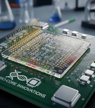
Harnessing Biochip IP for Enhanced Diagnostic Solutions
Biochip IP Technology drives innovation in diagnostics and biotechnology through protected, high-performance solutions, overcoming complexity with collaboration and unlocking broad benefits across multiple sectors.
EDITORIAL
The Next Wave of Semiconductor Innovation
As the semiconductor industry ventures into new frontiers, multiple technologies are converging to create systems that are more capable, efficient, compact and versatile.
In this edition of Semiconductor Review, we examine how semiconductors are evolving from mere computational engines into critical drivers of entirely new experiences, touching everything from healthcare to immersive media.
By embedding biosensing capabilities directly onto silicon, Biochip IP technology is transforming diagnostics, allowing real-time health monitoring at the molecular level. This integration into both consumer and clinical devices points to a future where medicine becomes increasingly predictive, personalized and seamlessly connected to everyday life.
In advanced optoelectronics, breakthroughs in nanoscale light control and novel materials are accelerating data transfer while improving energy efficiency and imaging precision. When combined with high-purity metals and compounds, these devices deliver higher conductivity, cleaner interfaces and lower defect densities—essential for next-generation 3D architectures and quantum-scale circuits that power everything from AI computing to sophisticated sensors.
High-speed CMOS image sensors are raising the bar for visual perception, allowing autonomous vehicles, industrial robots and smart devices to process information with unprecedented speed and accuracy. In parallel, microdisplay technologies are redefining human-computer interaction, making AR/VR systems lighter, brighter and more immersive while opening doors to compact optical solutions for consumer and enterprise applications.
Collectively, these advancements highlight a pivotal shift in the semiconductor landscape; from being measured purely by performance metrics to being valued for their transformative potential. Beyond raw power or speed, the industry’s future hinges on how intelligently silicon can bridge the digital and human worlds, creating devices and systems that enrich everyday life.
We hope this edition of Semiconductor Review helps you find the right partner for your business requirements.
This content is copyright protected
However, if you would like to share the information in this article, you may use the link below:
https://www.semiconductorreviewapac.com/edition/november-2025-27.html