
Thank you for Subscribing to Semiconductor Review Weekly Brief
× 
Semi Conductor Review Weekly Brief
Be first to read the latest tech news, Industry Leader's Insights, and CIO interviews of medium and large enterprises exclusively from Semi Conductor Review
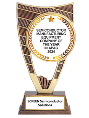
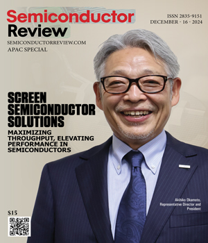
SCREEN Semiconductor Solutions has been recognized by Semiconductor Review Magazine as “Semiconductor Manufacturing Equipment Company of the Year in APAC -2024” based on our proprietary methodology, reflecting its position in the industry. This profile has been developed by the Semiconductor Review research and editorial team based on insights from an interview with Akihiko Okamoto, Representative Director and President.




 Akihiko Okamoto, Representative Director and President
Since entering the semiconductor equipment market in 1975, SCREEN has consistently set performance and customer satisfaction benchmarks.
With the No. 1 global market share in semiconductor cleaning processes, SCREEN has built its reputation on core technologies— etching, photolithography and image processing—refined over decades. This expertise has translated into a portfolio of high performance equipment that caters to both advanced device manufacturers and the burgeoning IoT and automotive devices, where specialized wafer sizes below 200mm are critical.
Collaborations with globally renowned research hubs like the Interuniversity Microelectronics Center (IMEC) and CEA-Leti, as well as strategic partnerships with leading academic institutions and industry innovators, help SCREEN in its dedication to consistently push the boundaries of what’s possible in semiconductor manufacturing.
“Our products are designed with the future in mind, enabling manufacturers to meet today’s demands while preparing for tomorrow’s challenges,” explains Akihiko Okamoto, representative director and president. “But at SCREEN, we don’t just sell equipment. We build relationships.”
Customers who choose SCREEN initially for its industryleading performance often return for the reliability and peace of mind that come with its comprehensive support ecosystem.
Performance You Can Count On, Reliability You Can Trust
At its core, the SU-3400 incorporates reconfigured wafer transport robots and redesigned processing chambers that reduce delays during wafer transitions. This precision engineering boosts processing capacity to an industry-leading 1,200 wafers per hour. By matching the processing capacity of batch-type systems while offering superior cleaning performance, it makes sure manufacturers can handle high-volume production with ease.
The SU-3400 single wafer cleaner, introduced in 2022, is a clear reflection of SCREEN Semiconductor Solutions’ commitment to innovation and efficiency. Built to tackle the challenges of modern semiconductor manufacturing, it strikes the perfect balance between high productivity, advanced processing capabilities and sustainable design.
-
Our products are designed with the future in mind, enabling manufacturers to meet today’s demands while preparing for tomorrow’s challenges
At its core, the SU-3400 incorporates reconfigured wafer transport robots and redesigned processing chambers that reduce delays during wafer transitions. This precision engineering boosts processing capacity to an industry-leading 1,200 wafers per hour. By matching the processing capacity of batch-type systems while offering superior cleaning performance, it makes sure manufacturers can handle high-volume production with ease.
The cleaner’s design also addresses factory space challenges. By reducing the size of its processing chambers and introducing a compact six-tiered tower structure, SCREEN has cut the equipment footprint by 30 percent. A smaller footprint doesn’t just save space; it simplifies factory layouts, streamlining workflows and minimizing production bottlenecks.
The SU-3400’s sustainability performance is another standout feature. Its environmental impact has been significantly reduced through advanced innovations such as fully automated airflow control and an improved cleaning nozzle and chemical circulation system. These enhancements reduced the equipment’s environmental impact (exhaust/nitrogen/chemical) by 20 percent.
These high-level productivity features have earned SU-3400 the 2023 Nikkei Business Daily Award, solidifying its position as transformative equipment for single-wafer cleaning.
In addition, SCREEN’s Coat/Develop Track equipment is capable of advanced applications like AI and high-performance computing. Its DT-3000, for instance, ensures precise photoresist application while minimizing particle contamination and is capable of handling advanced lithography processes.
SCREEN’s innovation extends to the annealing process as well. Traditional annealing often struggles with temperature control, leading to stress on delicate wafer layers. SCREEN’s flash lamp annealing equipment uses xenon flash lamp technology to deliver intense, millisecond-long pulses of light. This breakthrough reduces thermal stress while activating impurities in wafers, ensuring devices are optimized for performance.
The power of AI is also leveraged through its proprietary SCRAIS system, an innovative AI-based false report filtering tool embedded in its wafer inspection equipment. Using high-resolution image recognition, SCRAIS streamlines defect detection, reducing labor demands, cutting costs and boosting operational yields. Combining cutting-edge AI with its state-of-the-art inspection systems helps manufacturers achieve exceptional output quality with reduced effort.
World-Class Training and Support
Customer support isn’t an afterthought at SCREEN. It’s the foundation of everything it does. Take, for instance, SCREEN’s Global Training Center, TAKUMI, located in Kumamoto. This state-of-the-art facility offers an immersive training experience, guiding customers through the intricacies of equipment setup, maintenance, and modifications. The hands-on program is designed not just to instruct but to instill confidence, empowering users to maximize the potential of SCREEN’s advanced solutions.
This excellence is reinforced by field service-trained engineers, who provide on-site support for installation, setup and ongoing maintenance. For customers who require greater flexibility, SCREEN leverages remote training technologies like HoloLens, enabling real-time, interactive guidance regardless of location. With additional training centers in key regions such as the U.S., China and Germany, SCREEN makes sure expert assistance is always within reach.
The Process Technology Center in Hikone is equipped with a cleanroom dedicated to improving the efficiency and advancement of semiconductor manufacturing equipment. The center helps customers collaborate with technical managers to accelerate joint process development.
The blend of world-class training, on-site expertise and workflow optimization provides manufacturers the partnership and support they need to thrive in an ever-changing industry.
Living the Vision, Keeping the Promise
SCREEN’s journey into its next chapter of innovation is firmly rooted in sustainability, and it is shaping the future of semiconductor manufacturing.
As an active member of the Semiconductor Climate Consortium, established by SEMI and the imec SSTS program, SCREEN collaborates with global leaders to drive environmentally conscious advancements. Key initiatives include the Water Management Application at the Hikone Process Technology Center—now expanding site-wide to enhance water resource efficiency—and the implementation of Zeroboard, a CO₂ emission calculation and visualization cloud service designed to empower actionable environmental impact reduction.
But these initiatives are only part of the story. SCREEN has launched the SS-3200 for 200mm, a high throughput 200m wafer cleaning system that extends its world-leading spin scrubber lineup. This system addresses evolving customer needs while prioritizing eco-efficiency.
Such innovations do not go unnoticed. SCREEN has earned significant recognition. At the 70th annual award ceremony sponsored by the Okochi Foundation, SCREEN was honored with the prestigious Okochi Memorial Production Prize. Honored with the Excellent Performance Award in the categories of ‘Excellent Contribution in Green Manufacturing’ and ‘Excellent Production Support’ by Taiwan Semiconductor Manufacturing Company (TSMC) underscores SCREEN’s commitment to supplying equipment that reduces environmental impact while providing exceptional production support.
Sustainability has become a defining element of SCREEN’s ethos, a fact exemplified by its Micron Supplier Award 2024 for Outstanding Performance in Sustainability. Actively participating in Micron’s Scope 3 greenhouse gas emission reduction program, SCREEN has helped them achieve a 45 percent reduction in greenhouse gas emissions since 2019. SCREEN also achieved nearperfect scores in its RBA audits for its two manufacturing sites.
SCREEN’s impact continues to resonate globally, as it was selected among Europe’s top 10 semiconductor manufacturing solutions providers as well. These honors serve as milestones on SCREEN’s journey to shape the future of the semiconductor landscape.
“Reflecting on the road we’ve traveled, along with our developmental plans for the future, we remain committed to manufacturing industry-leading performance equipment that keeps our customers’ innovation and production always a step ahead in the fast-paced world,” concludes Okamoto.
| Share this Article:Tweet
|
Company
SCREEN Semiconductor Solutions
Management
Akihiko Okamoto, Representative Director and President
Description
SCREEN Semiconductor Solutions blends cutting-edge technology with reliability to remain an essential partner for manufacturers worldwide. Since entering the semiconductor equipment market in 1975, SCREEN has consistently set performance and customer satisfaction benchmarks. With a global market share in semiconductor cleaning processes, SCREEN offers a diverse lineup of cleaning, coat/develop track, annealing, inspection and metrology equipment.
This content is copyright protected
However, if you would like to share the information in this article, you may use the link below:
https://www.semiconductorreviewapac.com/screen-semiconductor-solutions