
SEMICONDUCTOR REVIEW THANK YOU FOR SUBSCRIBING
× 
Semi Conductor Review Weekly Brief
Be first to read the latest tech news, Industry Leader's Insights, and CIO interviews of medium and large enterprises exclusively from Semi Conductor Review
Semiconductor Review: Specials Magazine

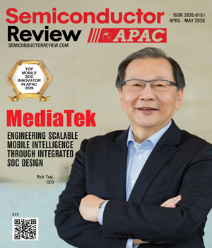
MediaTek
Engineering Scalable Mobile Intelligence through Integrated SoC Design
Smartphones today must process graphics, AI workloads, and high-speed connectivity within compact silicon footprints, where coordination between subsystems directly shapes user experience. MediaTek approaches this requirement through integrated system-on-chip architectures that unify compute, graphics, AI acceleration, and connectivity into coordinated silicon platforms. Its design ensures efficient data movement across subsystems, enabling devices to execute complex tasks with stability across varied usage scenarios. MediaTek’s Dimensity and Helio platforms reflect this integration by combining CPU clusters, GPU cores, AI processing units, and modem subsystems within a single die. This structure allows device manufacturers to deploy complete computing platforms without assembling multiple discrete components. The result is a streamlined hardware design that improves signal flow, reduces latency between subsystems, and supports stable device behavior under varying workloads. Structuring Compute Architecture for Balanced Workloads MediaTek designs its SoCs using multi-core CPU architectures that distribute workloads across performance and efficiency cores. This configuration enables the system to allocate tasks dynamically based on demand, ensuring that background processes and intensive applications are handled without resource contention. Graphics processing units within the SoC are optimized for rendering tasks such as gaming and video playback. These GPUs support high frame rates and visual fidelity while maintaining controlled power consumption. This balance allows devices to sustain graphics performance during extended sessions without thermal degradation. Memory subsystems are integrated to support high-bandwidth data access, enabling faster communication between processing units. This design ensures that applications requiring rapid data retrieval, such as gaming engines and multimedia processing, can operate without bottlenecks. The coordination between compute and memory strengthens overall system responsiveness.
Wafer
Ultratrend Technologies
Engineering Bulk AlN for Advanced Semiconductor Platforms
Dr. Liang WU, Founder and CEO
Why is bulk AlN industrialization critical for ultra-wide bandgap semiconductors? Industrializing bulk aluminum nitride (AlN) single-crystal substrates is one of the most technically demanding challenges in the ultra-wide bandgap (UWBG) semiconductor field. Ultratrend Technologies was founded in 2018 to address this challenge directly, focusing on bringing bulk AlN substrates into real device manufacturing. Headquartered in Hangzhou, the high-tech company was established by senior semiconductor experts who recognized that the future of UWBG electronics depends on substrate materials capable of sustaining extreme electrical, thermal and environmental demands. Rather than treating AlN as an experimental material, Ultratrend built full fabrication capability from the outset. Its scope spans reactor and hotzone design, modeling and simulation, process optimization, crystal growth, wafering and material characterization. Ultratrend has more than 60 patents applied for and granted, reflecting the depth of proprietary knowledge embedded across its technology stack. “Bulk AlN growth is not only about producing crystals, but about ensuring they can be consistently adopted in real device manufacturing,” says Dr. Liang Wu, Founder and CEO. Mastering Bulk AlN Growth What technical barriers define scalable bulk AlN crystal growth? AIN occupies a distinctive position within the UWBG semiconductor family. With an ultra-wide bandgap of 6.2 eV, an exceptionally high critical breakdown field, high thermal conductivity and semi-insulating resistivity, AlN ranks among the top when compared with emerging UWBG materials. These characteristics position it as a foundational substrate for deep-ultraviolet optoelectronics, high-power and high-frequency RF devices and next-generation power electronics. However, translating these intrinsic advantages into manufacturable substrates remains complex. Bulk AlN growth requires extreme thermal conditions and precise control of carbon and oxygen impurities, which directly impact DUV transparency. Ultratrend’s differentiation lies in how it addresses these challenges at system and process levels. The company has strategically adopted tungsten-based growth systems to minimize carbon and oxygen contamination, combined with homoepitaxial growth pathways to maintain crystal integrity. This strategy is supported by a multidisciplinary R&D team spanning materials science, computational modeling and equipment engineering. Ultratrend’s proprietary finite-element simulation platform integrates flow and mass transfer modeling, impurity transport, supersaturation control and three-dimensional stress prediction. These tools are embedded in equipment and process design to shorten development cycles and reduce growth risk. Multiple generations of fully automated physical vapor transport growth reactors, incorporating tailored hotzones and proprietary processes, have enabled stable material transport and suppression of parasitic nucleation. The outcome is consistent production of high-structural-quality AlN crystals with industry-leading deep-UV transparency. In 2024, Ultratrend introduced 2-inch high-transparency bulk AlN substrates demonstrating absorption coefficients of 7.2–10.7 cm⁻¹ in the 220–240 nm range and as low as 6.1 cm⁻¹ at 265 nm. For the first time, 2-inch PVT-grown AlN substrates achieved DUV transmittance comparable to HVPE-AlN, marking a significant milestone in bulk crystal growth..

Semiconductor Testing

Established in 1988 and based in Hidaka City, Saitama, Japan, JMT Inc.. has carved out a strong reputation in the semiconductor testing sector. The company specializes in manufacturing test sockets and sheets, with a particular focus on the use of silicone rubber materials. These components play a crucial role in the post-assembly phase of semiconductor devices, where they are used to assess the performance and durability of chips. At the core of JMT’s success is its ability to create highly customizable solutions for its clients. The company’s deep knowledge of silicone rubber allows it to produce components that deliver reliable performance even in the harshest testing environments, such as extreme temperatures. This ability to adapt and meet clients’ specific needs has made JMT a trusted partner for some of the world’s leading semiconductor companies, including Samsung, SK Hynix, and Micron. Offering Strong Balance of Cost Efficiency and Reliability JMT’s flagship product, the pressure-type conductive contact sheet PCR®, is a sheet-type contactor made primarily from silicone rubber. The use of silicone rubber enables stable electrical connections without damaging IC packages or test boards, making it well-suited for repeated use. PCR® offers a strong balance of cost efficiency and reliability, making it ideal for testing a wide range of semiconductor package types. PCR® features a unique internal structure in which conductive particles are aligned vertically through the thickness of the sheet. When pressure is applied to the electrode area containing these particles, they come into contact with one another, forming multiple current paths. This structure ensures stable electrical properties and enables accurate, reliable measurements. Additionally, PCR® utilizes a planar contact structure, which provides a wide tolerance range for positional errors and can flexibly accommodate minor misalignments. Its ability to connect over very short distances also makes it ideal for testing high-end products that require high-frequency performance. High-performance test sockets that incorporate the PCR® sheet-type contactor support a wide range of applications—from fine-pitch, small ICs to large, advanced packages. The simple structure of PCR® enables easy maintenance and user-friendly handling. Moreover, the socket’s pressureapplication mechanism can be customized to match each customer’s product specifications and testing environment, with structural options including clamshell, double-latch, and screw-fixed types. Taking a Customer-First Approac JMT’s commitment to customer satisfaction is another cornerstone of its business. The company goes beyond simply selling products; it listens carefully to its clients’ needs and tailors its solutions to meet them.
Testing and Quality Assurance

Unlocking the true value of Data - Lessons from the journey
Adarsha Marpalli, Sr Director- Global Head Data and Insights, Nexperia
Sensor

Industry 4.0: Navigating Disruptive Technologies in Manufacturing
Peter Chambers, Senior Director, OEM Sales APJ & Country Manager, Australia, AMD [NASDAQ: AMD]
Testing and Quality Assurance

Driving innovation in the Semiconductor Space
Rohit Vidwans, Executive Vice President Engineering, Ampere Computing
Intellectual Property

Harnessing the Power of Additive Manufacturing to Advance Semiconductor Capital Equipment Performance
Scott Green, Director Advanced Software R&D, 3D Systems Corporation
Semiconductor AI
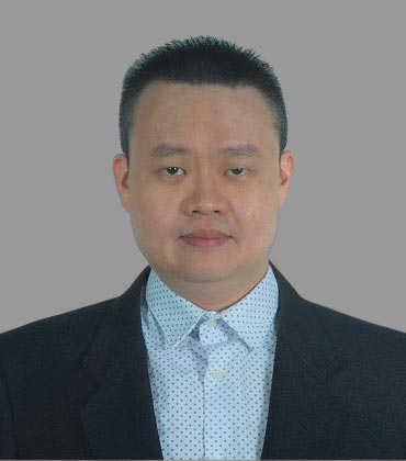
A Paradigm Shift: Leveraging Artificial Intelligence and Machine Learning in Design Engineering
Matthew Yap, Associate Director, Microchip Technology Inc

IN MY OPINION
Sensor
The Future of Code Storage
Frederick Chen, Sr. Technology Manager - Advanced Technology Development, Winbond

LAST WORD
Semiconductor Manufacturing
The Evolution of Insulated Gate Bipolar Transistors
Michele (Mike) Giulianini, Engineering Manager, Origin Energy
IN FOCUS

Future-Proofing Semiconductor Manufacturing in APAC: Strategies and Innovations
Semiconductor manufacturing in the APAC region faces challenges related to production complexity, supply chain issues, and sustainability concerns, but technological advancements offer significant opportunities.
EDITORIAL
Advancing Semiconductor Materials and Engineering Intelligence
The semiconductor industry continues to evolve as new materials, advanced design methodologies and sensing technologies expand the boundaries of electronic systems. In this edition of Semiconductor Review APAC, we examine how innovation across materials engineering and semiconductor design is shaping the next generation of high-performance devices and scalable technology platforms.
Our cover story features Ultratrend Technologies, recognized as the Top AlN Single Crystal Wafer Substrate Manufacturer in Asia 2026. The company has focused on industrializing bulk aluminum nitride (AlN) substrates, a material at the forefront of ultra-wide-bandgap semiconductor development. Through its integrated approach spanning reactor design, simulation, crystal growth and wafer processing, Utrendtech has built a complete fabrication capability to support real device manufacturing. Its proprietary growth systems and simulation platforms enable precise control of impurities and crystal quality, producing high-transparency AlN substrates suitable for deep-ultraviolet optoelectronics, RF systems and next-generation power electronics. By combining materials science expertise with scalable production processes, the company is advancing the practical adoption of AlN substrates within the semiconductor ecosystem.
Complementing this focus on materials innovation, this issue also explores broader engineering and technology trends shaping the semiconductor sector. These developments reflect the industry’s ongoing effort to balance performance scaling, manufacturing complexity and system reliability while enabling new device architectures and application domains.
Leadership insights further enrich this discussion. Matthew Yap, Associate Director at Microchip Technology Inc., examines how artificial intelligence and machine learning are transforming semiconductor design engineering by improving productivity, enabling engineers to manage larger design blocks and supporting automated optimization workflows. Meanwhile, Joshua R. Windmiller, PhD, CLP, SM-IEEE, Head of New Analytes and Sensing Platforms at Dexcom, Inc., shares perspectives on translating semiconductor-enabled sensing technologies into practical healthcare platforms, emphasizing the importance of designing innovations that address real patient needs and scale effectively in clinical environments.
Together, these perspectives highlight how advances in materials, engineering methods and sensing technologies are expanding the role of semiconductors across industries. We invite readers to explore the insights in this edition and engage with the ideas shaping the future of semiconductor innovation.
This content is copyright protected
However, if you would like to share the information in this article, you may use the link below:
https://www.semiconductorreviewapac.com/edition/april-may-2026-37.html