
SEMICONDUCTOR REVIEW THANK YOU FOR SUBSCRIBING
× 
Semi Conductor Review Weekly Brief
Be first to read the latest tech news, Industry Leader's Insights, and CIO interviews of medium and large enterprises exclusively from Semi Conductor Review
Semiconductor Review: Specials Magazine
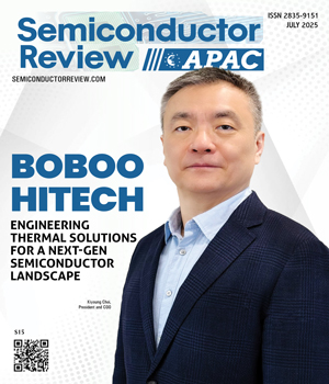
BOBOO HITECH
Engineering Thermal Solutions for a Next-Gen Semiconductor Landscape
BOBOO HITECH has spent over 30 years evolving from a components supplier into a vertically integrated company delivering advanced thermal and clamping solutions across semiconductor manufacturing. The company designs, manufactures, and supplies mission-critical heaters and electrostatic chucks (ESCs) that play vital roles at every stage of chip production. Its broad product portfolio includes metal and ceramic heaters for front-end deposition equipment, ESCs for etching, ion implantation, and deposition processes, and pulse and stage heaters tailored for advanced back-end packaging. BOBOO HITECH’s expertise in materials—from metals and advanced ceramics to polymer jackets—allows it to seamlessly bridge the front-end and back-end, a rare capability among component makers. A tightly integrated operational model supports this comprehensive product range. By consolidating research and development, manufacturing, quality assurance, and direct sales under one roof, BOBOO HITECH delivers highly customized, precision-engineered components with the speed and flexibility required by global semiconductor leaders. At the core of the company’s innovation is its multidisciplinary engineering team—true to its identity as engineers, specialists, and problem solvers. BOBOO HITECH’s ability to design components for harsh, high-load environments is rooted in this technical depth, ensuring each product meets demanding material and functional specifications. In addition to developing new solutions, the company also offers repair and refurbishment services, reinforcing its commitment to providing complete lifecycle support for semiconductor equipment makers and chip manufacturers worldwide.
Wafer
Shanxi Semisic Crystal Co., Ltd.. (hereafter called SEMISiC) has emerged as a globally recognized 'little giant' in the silicon carbide (SiC) arena with its production scale and technical expertise. Its success took root in 2009 when a seven-person team began researching silicon carbide (SiC) materials in a small lab. They started by developing their own SiC crystal growth equipment and then improving material quality through extensive experimentation and optimization of various growth factors. The journey took a major leap in 2018 when Tesla’s adoption of SiC power modules in the Model 3 validated the material’s potential from a technical as well as commercial perspective. This sparked a global race among automakers and semiconductor companies to scale SiC technology, accelerating SEMISiC’s growth and positioning in the market. “We were ready,” says Serena Sun, sales manager. “When the market shifted, we had the technology, the people and the equipment in place. All we had to do was expand and refine.” Today, its wafers, qualified by dozens of leading international power device manufacturers, are exported worldwide. Part of that success comes from SEMISiC’s ability to deliver real value to its customers. Clients consistently choose it for three core reasons: competitive pricing, technical flexibility and supply chain reliability. Its SiC substrates offer dependable quality with a cost advantage. Collaborating closely with device manufacturers, it tailors substrate solutions to specific design needs—adjusting crystal properties and process conditions to improve performance and simplify integration. In a market often disrupted by uneven supply, SEMISiC's in-house production systems and experienced manufacturing teams ensure stability and scalability.
Sensor

Rapidly Moving Market of Semiconductor Packaging
Cherie Sasan, Head of Design and Development, Power Module Technology, Integrated Micro- Electronics, Philippines [PSE: IMI]
Wafer

Scaling New Heights With AI in Silicon Wafer Manufacturing
J -Wing Teh, Director of Silicon & Systems Design Engineering, AMD [NASDAQ: AMD]
Wafer

Long-Standing Lean Thinking
Stewart Johnstone, Vice President Asia, Adient
Semiconductor Manufacturing

LG Legal Insights: Navigating today's Complex Business Landscape
Aini Amnia Majda, Head of Legal and Compliance, LG Electronics
Semiconductor Manufacturing

Pioneering A New Product Category in Medical Devices
Cecile Clavier, Global Director - Pediatric Business Unit, Hoya Vision Care

IN MY OPINION
Semiconductor Manufacturing
Building a Strong Collaborative Framework for Artificial Intelligence
Boon Siew Han, Regional Head of Humanoid Component Business & R&D (APAC & Greater China), Schaeffler

LAST WORD
Semiconductor Manufacturing
The Evolution of Insulated Gate Bipolar Transistors
Michele (Mike) Giulianini, Engineering Manager, Origin Energy
IN FOCUS
EDITORIAL
Building the Next Generation of Electronics
Silicon Carbide (SiC) is amid a significant shift in the semiconductor landscape as demand intensifies for more robust, energy-efficient solutions across power electronics and mobility applications. The industry is experiencing rapid expansion, through a confluence of technological advancements and market pressures that are reshaping how wafers are produced and how semiconductor equipment components are designed and manufactured.
One of the key drivers behind this surge is the electrification of transportation. As electric vehicles go mainstream, the need for materials that support higher voltages and temperatures with greater efficiency has placed SiC at the core of next-generation powertrain systems. This is accelerating innovation in wafer production as manufacturers push to meet both performance and volume demands.
At the same time, the industry's shift to 200mm SiC wafers is a major step in scaling. This evolution is redefining crystal growth and slicing processes while increasing the demands on equipment component manufacturers, whose precision parts must now perform reliably under more extreme and specialized conditions.
This edition of Semiconductor Review APAC brings recent developments in SiC wafer manufacturing and equipment component engineering into focus, highlighting the innovations, challenges and key players shaping the future of wide-bandgap semiconductor technology.
It features thought leadership articles from industry experts, including Stewart Johnstone, vice president Asia at Adient, who shares insights on leveraging lean manufacturing principles, decentralized operations, and emerging technologies to enhance agility, efficiency, and resilience across production networks. Dewi Fitriyati, head of business development, PT. KATOLEC INDONESIA delves into her strategies, principles, and insights on succeeding in business development within the fast-evolving electronics industry.
We hope this edition gives you valuable perspectives and practical insights to navigate the evolving demands of semiconductor manufacturing and electronics, while highlighting the innovations and strategies shaping the future of the industry.
This content is copyright protected
However, if you would like to share the information in this article, you may use the link below:
https://www.semiconductorreviewapac.com/edition/july-2025-17.html